
Hardware hacking: chip-off for beginners
Table of Contents
Introduction to hardware hacking
Before getting our hands dirty with hardware hacking, let’s start with a brief introduction to flash memories, a component that we will find very often in the PCBs we will analyze. Flash memories are read-mostly memory, designed as an improvement of the more traditional EEPROM memories. Flash memories can be found in a variety of electronic devices, including personal computers, appliances and pendrives. One of their most common applications is to serve as firmware storage, and therefore knowing how to dump its contents and analyze the resulting file is a desirable skill to the hardware hacker.
There are multiple ways to dump the contents of a flash memory. If we are lucky enough, the PCB under analysis may have open debug ports (JTAG, SWD…) that we could leverage to interact with the board and, in some cases, even letting us perform a step-by-step execution of the firmware and dump the memory to a file. In many other cases, however, these ports may be disabled or not exist whatsoever, but the flash memory itself may be extern and be exposed as a standalone component. In these cases, some EEPROM programmers feature a test clip that can be attached directly to the flash memory, without needing to desolder it from the board.
However, there are still cases in which the only way to go is to desolder the component from the board. These memories are usually surface mount devices (SMD), hence desoldering pumps may fall short. Even though the usage of solder wick with a soldering iron has been documented, this technique is highly limited by the size of the solder joints, being suitable for scenarios with big solder pads or THT components. In all other cases, using a hot air rework station is generally a more sensible solution.
In this post we describe how to phisically remove a flash memory from the board to extract its contents, a technique called “chip-off”, using a hot air rework station. We will use this technique in to two satellite TV FTA receivers analyzed during a previous investigation carried out by Tarlogic on IKS protocols and satellite TV piracy. In order to accomplish this, we will need:
- A hot air rework station: including a hot air gun and a preheating platform.
- Soldering tools: tweezers, magnifying glass and flux to clean the solder joints.
- A compatible flash / EEPROM programmer
Hardware hacking – Chip-off
Locating the memories
The first step is always to identify the integrated circuit encasing the flash memory we want to extract. As these memories tend to be indistinguishable from any other integrated circuit to the naked eye, it is convenient to look up the datasheet of any component suspect of being a flash memory. Normally, a simple search of the part number on Google will return the datasheet on the first result.
Operating a hot air station
The operation of hot air stations is simple: a jet of hot air (more than 200º C) is directed towards the component we want to extract, so that the solder joints melt and the component could be extracted with tweezers. However, parameters like air temperature, speed or the distance to the nozzle must be adjusted according to the component to extract.
Other important aspect to have in mind is the effect of differential heating on the board. When a jet of hot air is applied to a PCB at room temperature, most of the heat is diffused to the colder spots, making the heating of the region of interest inefficient. It could be tempting to increase the temperature of the jet. However, this is dangerous: the component is put under increased thermal stress and the temperature gradient increases along the board. The temperature difference on the board will produce different thermal expansion on different points, producing mechanical stress that may damage the board.
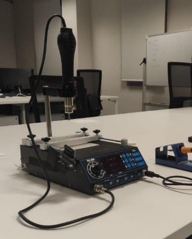
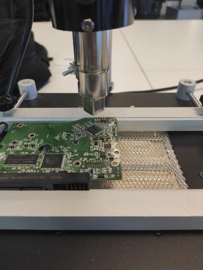
The alternative is to preheat the board, for which multiple techniques exist. In this example we will be using a MLINK H6 hot air rework station, which features an IR preheating board, on top of which the circuit board is placed.
In order to desolder a component from a PCB, we start by placing the board on the platform on top of the preheating plate and secure it by turning the platform screws, adjusting its position so that the jet of hot air falls right over the component we want to extract.
Next, we switch on the preheating plate, waiting for the preheating plate to reach the desired temperature. The optimal temperature depends on the component size, the solder material and the state of the circuit. In this case, some testing was performed on old boards extracting small components and integrated circuits.
For most small components, a preheating temperature of 240º C is enough. Older boards or boards with joints made of different solder alloys may need temperatures up to 280º C. In any case, the use of flux may help reduce the required temperature and prevent damage.
Bigger integrated circuits may need a somewhat higher temperature, ranging from 280º C to 300 ºC. In these cases, appropriately shaped and oriented hot air gun nozzles will always be of great help. In addition, adjusting the height at which the hot air gun is held has been found to be useful with components of bigger surface, although it must be handled with care to prevent dame on the surrounding components. In case the density of electronic components was too high, and directing the jet to a single component was unfeasible, we can cover the surrounding components with thermal tape to keep them from overheating.

Extracting the hardware components
Once the platform has reached the desired temperature, the hot air gun is switched. We keep the air jet flowing until the component can be extracted with the tweezers, up to a maximum of 20 – 30 seconds.
For smaller integrated circuits and other components, tweezers are placed vertically on the component, grabbing it without touching the pints. For bigger-sized components in which tweezers cannot ensure a safe grab, we may need to grab the component by a corner, without touching the pins and applying a soft pressure to extract it. The result must be clean, without leaving traces of track on the component pins.
Hardware hacking tools – Memory Dump
Choosing the programmer
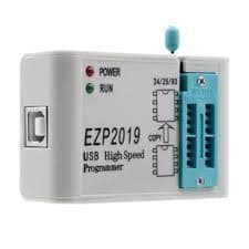
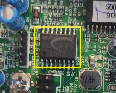
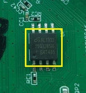
For the readout of the flash memories, the EEPROM programmer EZP2019+ was chosen because of its simplicity and low cost. Depending on the memory packaging, an appropriate adapter will be needed. In our case, a SOP16 300mil adapter was used for the Winbond (16 pin) memory, while a SOP8 209mil adapter was used for the GigaDevice memory (8 pins). The programmer package includes a CD with drivers and the required software in a ZIP file.
Let’s Get Hacking – Dumping the firmware
Every programmer has its peculiarities, and there is no simple tool that works for everything. In the case of the EZP2019, in addition to the installation of the software contained in the CD, the installation of the corresponding drivers was also needed. The tool (contained in the executable file EZP2019+.exe) reminds to a regular hexadecimal editor with various extra options to handle the programmer.
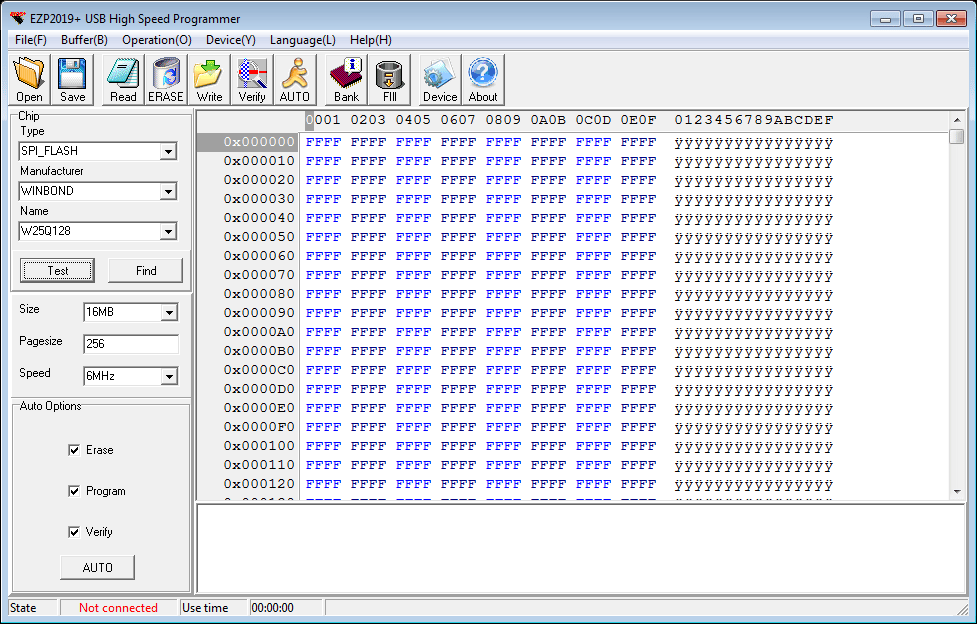
Fortunately, the memories we extracted are natively supported by the application, which will save the work of establishing the memory parameters manually. In this instance, we only needed to provide:
- Memory type: could be EEPROM, 24, 25 or 93 series, or a flash memory as described in this example.
- Manufacturer: Winbond and GigaDevice
- Model: W25Q128 and GD25Q32B respectively
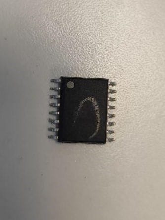
On the other hand, the lack of documentation of these devices is a great obstacle for their operation. Apart from the the warranty leaflet and a set of PDF manuals about the dump software (and not the programmer itself), no instructions regarding chip adapters were included. In particular, although in many cases the right adapter for each memory could be easily guessed (this was the case of the WinBond memory, as there was only one 16 pin adapter), the right orientation of the memory had to be deduced experimentally, increasing the risk of damaging the component.
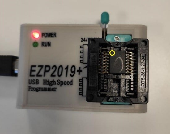
The conclusion was that the first pin, indicated by a round mark in one of the corners of the packaging, must be aligned to the adapter’s corner with a equivalent alignment mark on it, and the adapter must be connected to the programmer so that the mark is oriented towards the USB connector. The right orientation can be tested simply by clicking on the Test button of the memory dump software, which will prompt an error message in case the orientation was not correct.
Although the tool makes a good work self-configuring the readout parameters of the device, it is a good idea to verify that the size of the memory, the page size and the read speed are correct. These parameters can be found in the corresponding datasheet. In our case, the Winbond memory had a capacity of 16 MB and a page size of 256 bytes, while the GigaDevice memory had a capacity of 4 MB and a page size of 256 as well. In both cases, we confirmed that a read speed of 12 MHz produced no readout errors whatsoever.
In order to read the contents of the connected memory, we can simply click on the Read button in the application’s toolbar and, if all parameters were correct, the readout progress will be shown in the status bar.
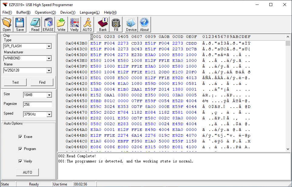
If the read speed is too high, the readout may fail and produce erroneous results. That’s why it is a good practice to verify the contents of the dumped data by clicking on Verify and visualize its contents on the main window. The dumped data can be saved to a file simply by clicking on Save.
Wrapping it up
Although we may think that storing the contents of the dumped to a file is the final step before proceeding to the reverse engineering of the firmware, some pre-analysis of the data may be desirable.
One of the first things we may want to verify is whether the firmware is compressed or encrypted, something we can do by running an entropy analysis with tools like binwalk. If the entropy is low in general, it could also be interesting to check the endianness of the data, as data words may be reversed if the endianness of the memory does not match the endianness of the embedded processor. We can do it by looking for ASCII strings in the firmware and attempt to read them. If the printable text is unreadable, but it is characterized by single capital letters in the middle of a word (things like “nihTl sg eokisiht.”), chances are that the endianness of words of some power of 2 is reversed.
Discover our work and cybersecurity services at www.tarlogic.com